Optional_resources
This part explains the inner working principle of the optical cube in depth, and you can check it selectively if you are interested!
schematic diagram
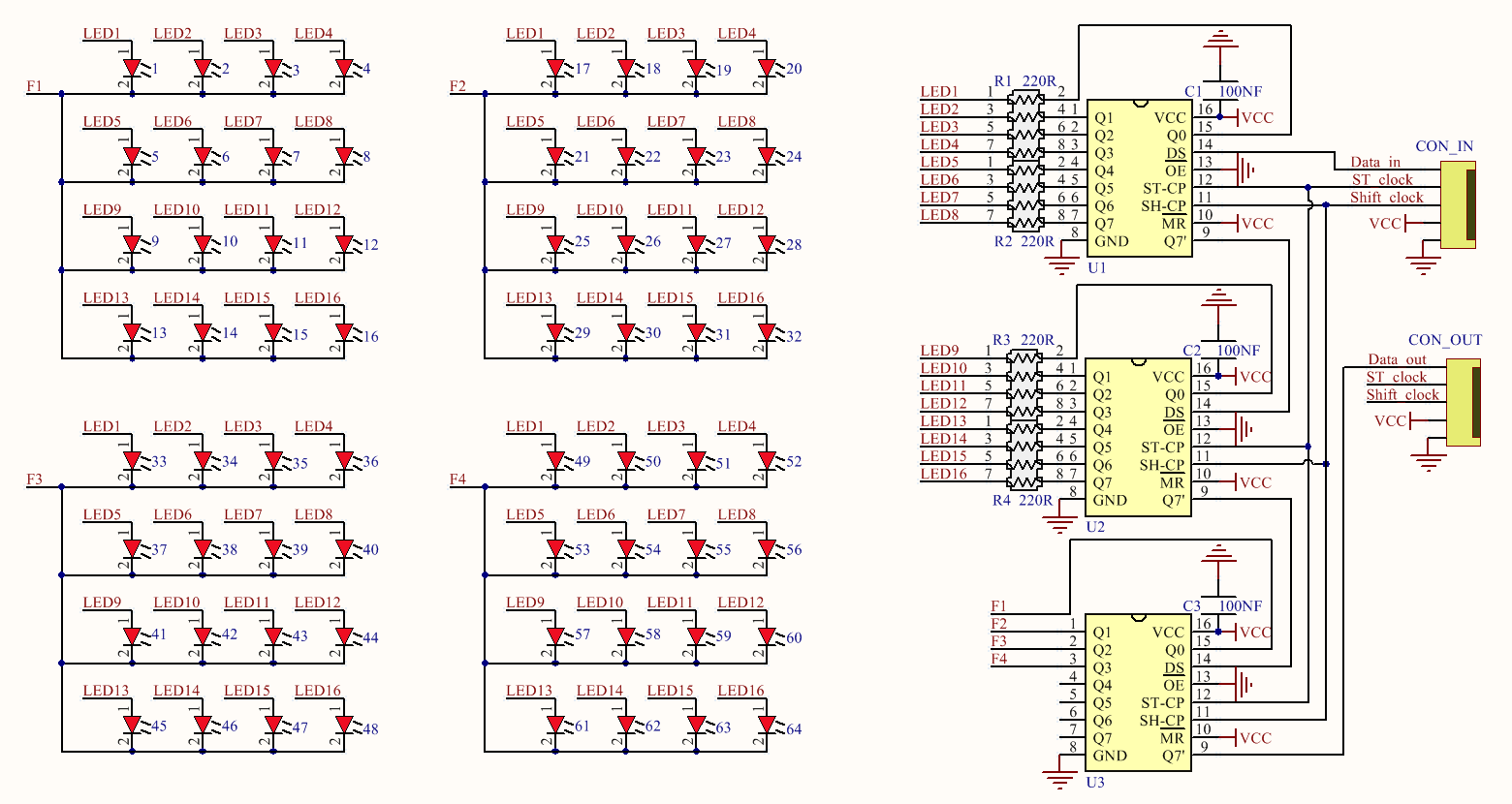
The light cube has 4 layers (F1, F2, F3, F4), each layer has 16 leds with common cathode wiring, which are controlled by 3 74HC595 serial to parallel data chips. Use the MCU’s timing interrupt function to turn on and off the leds in each layer (frequency ≥50Hz) to achieve control of all the leds in the cube.
74HC595.pdf
Communication data format
A data stream:
LEDs |
LEDs |
Layers |
|---|---|---|
16-15-14-13-12-11-10-9 |
8-7-6-5-4-3-2-1 |
F1-F2-F3-F4-1-1-1-1 |
D0-D1-D2-D3-D4-D5-D6-D7 |
D0-D1-D2-D3-D4-D5-D6-D7 |
D0-D1-D2-D3-1-1-1-1 |
“Dx”: 0 or 1.
A data stream entry protocol:
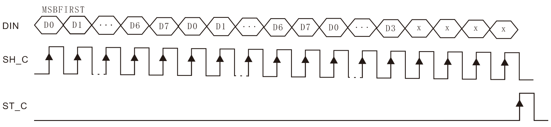
DIN = Data_in
ST_C = ST_clock
SH_C = Shift_clock, the recommended frequency is less than 25MHz.
Timing display format
A cube:
t |
t |
t |
t |
t |
…. |
t |
…. |
|---|---|---|---|---|---|---|---|
Laye 4 |
Laye 3 |
Laye 2 |
Laye 1 |
Laye 4 |
…. |
Laye 1 |
…. |
A data stream |
A data stream |
A data stream |
A data stream |
A data stream |
…. |
A data stream |
…. |
t: MCU timer interrupt time.
Cube display frequency: It must be ≥ 50Hz, f = 1s/(t * 4)
Series multiple cubes:
T |
T |
…. |
T |
T |
T |
…. |
|---|---|---|---|---|---|---|
Cube N |
Cube N-1 |
…. |
Cube 2 |
Cube 1 |
Cube N |
…. |
T: The MCU timer displays the time of a cube, T = (t*4).
Cube display frequency: It must be ≥ 50Hz, f = 1s/(T * N)
End!